
JSD PCB offers a wide range of different printed circuit boards to our customers in the world. We supply you the best quality, best price and heart to heart service.
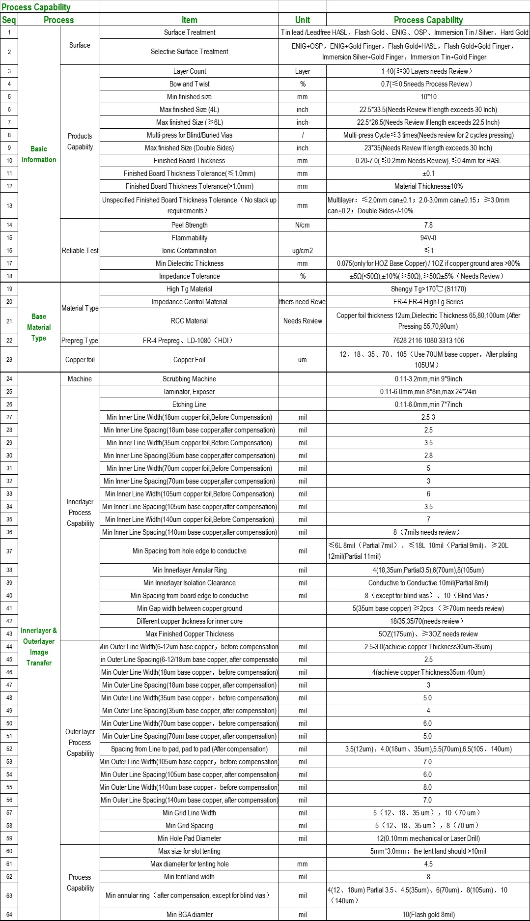
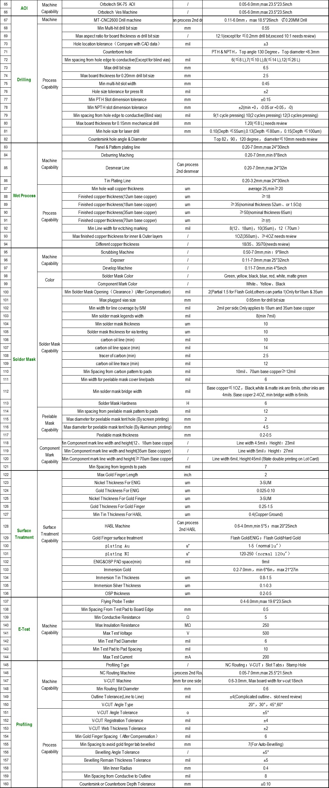
Surface treatment | HASL, Gold plating, Immersion gold,Immersion tin, Immersion silver, Gold fingers (Hard gold), OSP |
Count of layers | double-side to above 40 layers |
Min track width | 3mil (0.076mm) |
Min track space | 3mil (0.076mm) |
Min space between track to pad, pad to pad | 3mil (0.076mm) |
Minimum drill hole diameter | 6mil (0.15mm) mechanical drill; 4mil (laser drill); |
Min pads for vias | 12mil (0.3mm) |
Max aspect ratio | 0.052083333 |
Max PCB dimension | 23 x 35 inches (584.2 x 889.0mm) |
PCB thickness | 8.27-275.8mil (0.21-7.0mm) |
Max copper weight | 10 OZ |
Soldermask bridge between solder dam | 4mil (0.10mm) |
Minimum soldermask annular | 1.5mil (0.038mm) |
Soldermask colors | green, yellow, black, blue, matte, semi-matte, transparent LPI solder mask and peelable soldermask |
Plugged hole size | 0.15mm- 0.5mm |
Special material: | HTG FR4, high frequency (Rogers, Teflon, ARLON, TYCONIC), halogen free, different material mixing laminating |
Special techniques | blind and buried vias (min hole size is 0.1 mm), high layer with heavy copper |
Remark | the copper foil is 1OZ and 0.5OZ, If the copper foil is above 2OZ (including 2OZ), the above parameter will be changed. |

Copryright © 2017 JSD - All rights reserved.Made by Digood.